- 您现在的位置:买卖IC网 > Sheet目录2007 > LTC6900IS5#TR (Linear Technology)IC OSC SILICON 20MHZ TSOT23-5
LTC6900
3
6900fa
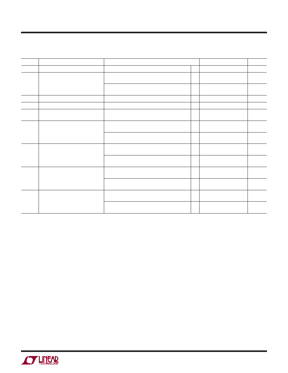
ELECTRICAL CHARACTERISTICS
Note 1: Stresses beyond those listed under Absolute Maximum Ratings
may cause permanent damage to the device. Exposure to any Absolute
Maximum Rating condition for extended periods may affect device
reliability and lifetime.
Note 2: Frequencies near 100kHz and 1MHz may be generated using two
different values of RSET (see the Selecting the Divider Setting Resistor
paragraph in the Applications Information section). For these frequencies,
the error is specied under the following assumption: 20k < RSET ≤ 200k.
Note 3: Frequency accuracy is dened as the deviation from the
fOSC equation.
Note 4: Jitter is the ratio of the peak-to-peak distribution of the period to
the mean of the period. This specication is based on characterization and
is not 100% tested. Also, see the Peak-to-Peak Jitter vs Output Frequency
curve in the Typical Performance Characteristics section.
The
l denotes the specications which apply over the full operating
temperature range, otherwise specications are at TA = 25°C. V+ = 2.7V to 5.5V, RL= 5k, CL = 5pF, Pin 4 = V + unless otherwise noted.
All voltages are with respect to GND.
SYMBOL
PARAMETER
CONDITIONS
MIN
TYP
MAX
UNITS
V+
Operating Supply Range
●
2.7
5.5
V
IS
Power Supply Current
RSET = 400k, Pin 4 = V+, RL = ∞
V+ = 5V
fOSC = 5kHz
V+ = 3V
●
0.32
0.29
0.42
0.38
mA
RSET = 20k, Pin 4 = 0V, RL = ∞
V+ = 5V
fOSC = 10MHz
V+ = 3V
●
0.92
0.68
1.20
0.86
mA
VIH
High Level DIV Input Voltage
●
V+ – 0.4
V
VIL
Low Level DIV Input Voltage
●
0.5
V
IDIV
DIV Input Current (Note 5)
Pin 4 = V+
V+ = 5V
Pin 4 = 0V
V+ = 5V
●
–4
2
–2
4μA
μA
VOH
High Level Output Voltage (Note 5)
V+ = 5V
IOH = – 1mA
IOH = –4mA
●
4.8
4.5
4.95
4.8
V
V+ = 3V
IOH = – 1mA
IOH = –4mA
●
2.7
2.2
2.9
2.6
V
VOL
Low Level Output Voltage (Note 5)
V+ = 5V
IOL = 1mA
IOL = 4mA
●
0.05
0.2
0.15
0.4
V
V+ = 3V
IOL = 1mA
IOL = 4mA
●
0.1
0.4
0.3
0.7
V
tr
OUT Rise Time
(Note 6)
V+ = 5V
Pin 4 = V+ or Floating, RL = ∞
Pin 4 = 0V, RL = ∞
14
7
ns
V+ = 3V
Pin 4 = V+ or Floating, RL = ∞
Pin 4 = 0V, RL = ∞
19
11
ns
tf
OUT Fall Time
(Note 6)
V+ = 5V
Pin 4 = V+ or Floating, RL = ∞
Pin 4 = 0V, RL = ∞
13
6
ns
V+ = 3V
Pin 4 = V+ or Floating, RL = ∞
Pin 4 = 0V, RL = ∞
19
10
ns
Note 5: To conform with the Logic IC Standard convention, current out of
a pin is arbitrarily given as a negative value.
Note 6: Output rise and fall times are measured between the 10% and 90%
power supply levels. These specications are based on characterization.
Note 7: Guaranteed by 5V test.
Note 8: The LTC6900C is guaranteed to meet specied performance from
0°C to 70°C. The LTC6900C is designed, characterized and expected to
meet specied performance from – 40°C to 85°C but is not tested or
QA sampled at these temperatures. The LTC6900I is guaranteed to meet
specied performance from –40°C to 85°C.
发布紧急采购,3分钟左右您将得到回复。
相关PDF资料
LTC6902IMS#TRPBF
IC OSC SILICON 20MHZ 10MSOP
LTC6904MPMS8#TRPBF
IC OSC SILICON 68MHZ 8MSOP
LTC6905HS5-133#TRPBF
IC OSC SILICON 133MHZ TSOT23-5
LTC6905MPS5#TRPBF
IC OSC SILICON 170MHZ TSOT23-5
LTC6906HS6#TRPBF
IC OSC SILICON 1MHZ TSOT23-6
LTC6907HS6#TRPBF
IC OSC SILICON 4MHZ TSOT23-6
LTC6908HS6-2#TRPBF
IC OSC SILICON 10MHZ TSOT23-6
LTC6909HMS#TRPBF
IC OSC SILICON 6.67MHZ 16-MSOP
相关代理商/技术参数
LTC6900IS5#TRM
功能描述:IC OSC SILICON 20MHZ TSOT23-5 RoHS:否 类别:集成电路 (IC) >> 时钟/计时 - 可编程计时器和振荡器 系列:- 产品培训模块:Lead (SnPb) Finish for COTS
Obsolescence Mitigation Program 标准包装:45 系列:- 类型:温度 - 补偿晶体振荡器(TCXO) 计数:- 频率:25MHz 电源电压:3.135 V ~ 3.465 V 电流 - 电源:1.5mA 工作温度:-40°C ~ 85°C 封装/外壳:16-SOIC(0.295",7.50mm 宽) 包装:管件 供应商设备封装:16-SOIC W 安装类型:表面贴装
LTC6900IS5#TRMPBF
功能描述:IC OSC SILICON 20MHZ TSOT23-5 RoHS:是 类别:集成电路 (IC) >> 时钟/计时 - 可编程计时器和振荡器 系列:- 标准包装:3,000 系列:- 类型:振荡器 - 晶体 计数:- 频率:- 电源电压:2.3 V ~ 5.5 V 电流 - 电源:1.07mA 工作温度:-30°C ~ 80°C 封装/外壳:SOT-665 包装:带卷 (TR) 供应商设备封装:SS迷你型-5D 安装类型:表面贴装 其它名称:AN8955SSMTXLTR
LTC6900IS5#TRPBF
功能描述:IC OSC SILICON 20MHZ TSOT23-5 RoHS:是 类别:集成电路 (IC) >> 时钟/计时 - 可编程计时器和振荡器 系列:- 产品培训模块:Lead (SnPb) Finish for COTS
Obsolescence Mitigation Program 标准包装:45 系列:- 类型:温度 - 补偿晶体振荡器(TCXO) 计数:- 频率:25MHz 电源电压:3.135 V ~ 3.465 V 电流 - 电源:1.5mA 工作温度:-40°C ~ 85°C 封装/外壳:16-SOIC(0.295",7.50mm 宽) 包装:管件 供应商设备封装:16-SOIC W 安装类型:表面贴装
LTC6900IS5TRMPBF
制造商:Linear Technology 功能描述:Resistor Set Oscillator 20MHz TSOT23-5
LTC6902
制造商:LINER 制造商全称:Linear Technology 功能描述:Multiphase Oscillator with Spread Spectrum Frequency Modulation
LTC6902CMS
功能描述:IC OSC SILICON 20MHZ 10MSOP RoHS:否 类别:集成电路 (IC) >> 时钟/计时 - 可编程计时器和振荡器 系列:- 产品培训模块:Lead (SnPb) Finish for COTS
Obsolescence Mitigation Program 标准包装:45 系列:- 类型:温度 - 补偿晶体振荡器(TCXO) 计数:- 频率:25MHz 电源电压:3.135 V ~ 3.465 V 电流 - 电源:1.5mA 工作温度:-40°C ~ 85°C 封装/外壳:16-SOIC(0.295",7.50mm 宽) 包装:管件 供应商设备封装:16-SOIC W 安装类型:表面贴装
LTC6902CMS#PBF
功能描述:IC OSC SILICON 20MHZ 10MSOP RoHS:是 类别:集成电路 (IC) >> 时钟/计时 - 可编程计时器和振荡器 系列:- 标准包装:3,000 系列:- 类型:振荡器 - 晶体 计数:- 频率:- 电源电压:2.3 V ~ 5.5 V 电流 - 电源:1.07mA 工作温度:-30°C ~ 80°C 封装/外壳:SOT-665 包装:带卷 (TR) 供应商设备封装:SS迷你型-5D 安装类型:表面贴装 其它名称:AN8955SSMTXLTR
LTC6902CMS#PBF
制造商:Linear Technology 功能描述:Programmable Oscillator IC